Lab 7 - ECE 421L
Authored
by Leanna Guevara, guevaral@unlv.nevada.edu
October 27, 2014
Using buses and arrays in the design of word inverters, muxes, and high-speed adders
8-Bit Inverter
Schematic
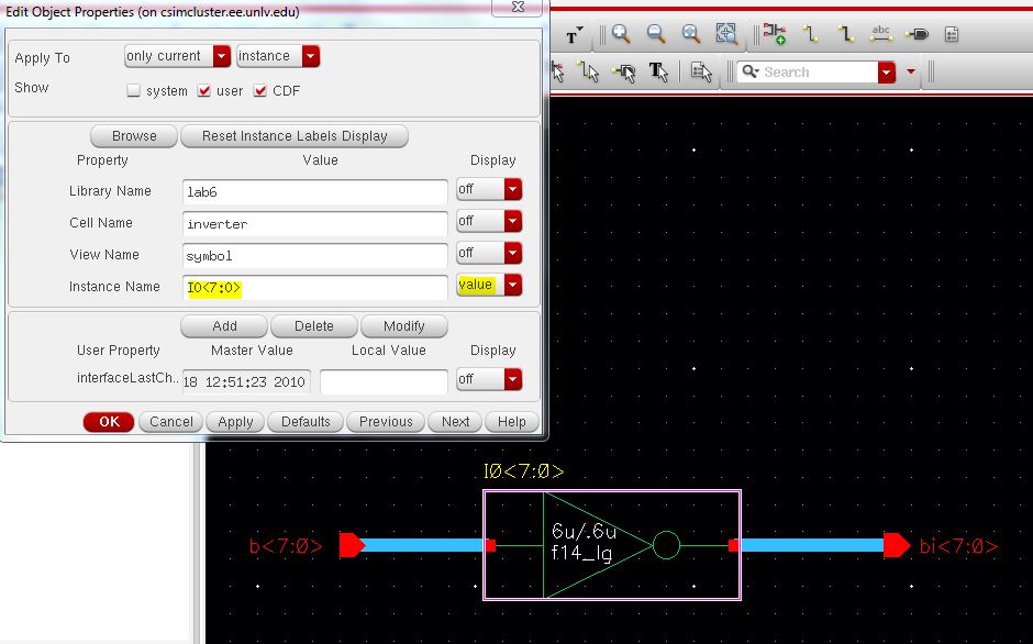
- Input <7:0> to signify 8-bits
- Use shift+w for a thick wire
- Check and save before creating a new symbol
Symbol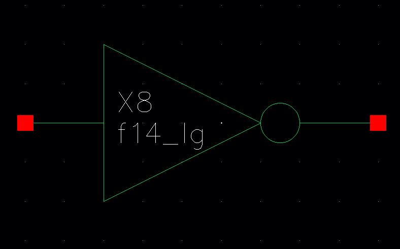
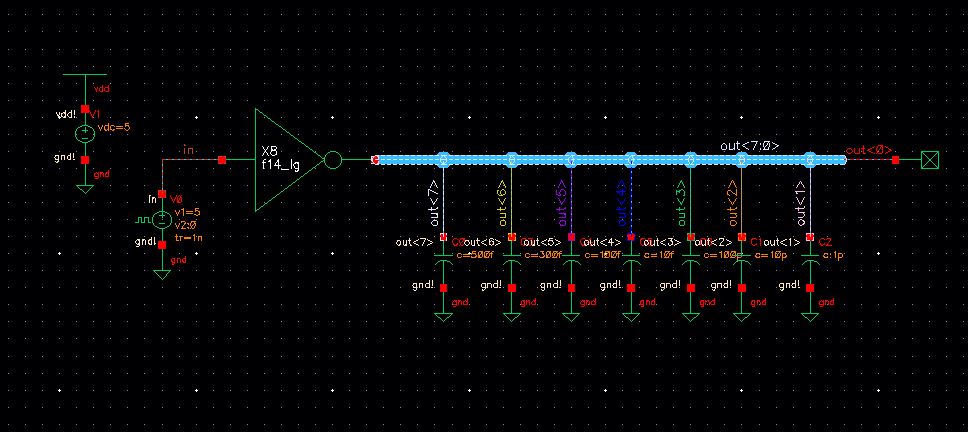
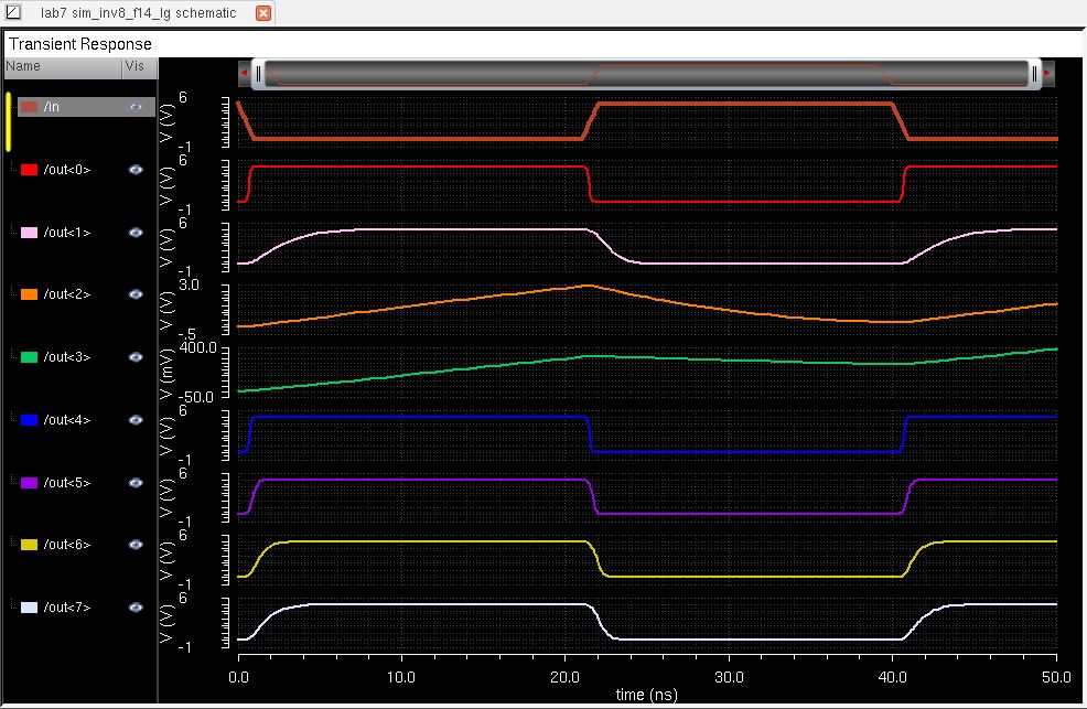
Simulations
The simulation will not work if the inverter is not connected to 8 outputs with a thick wire.
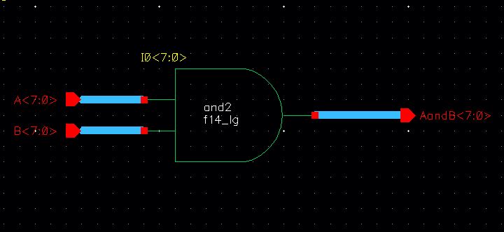
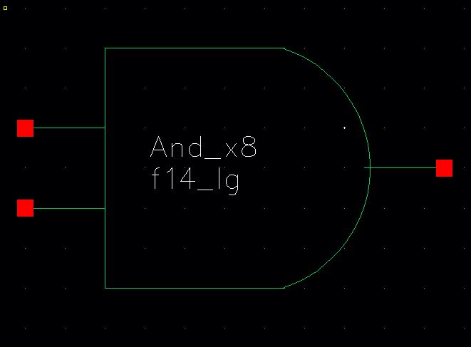
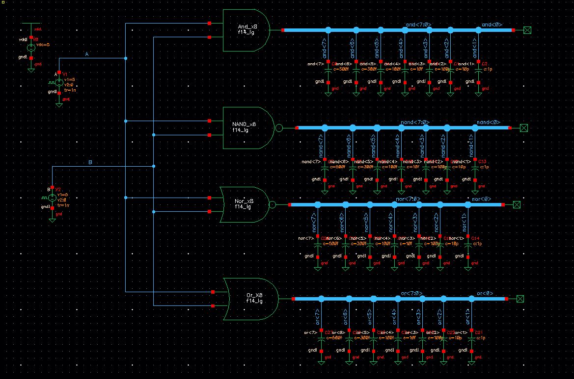
8-bit AND
Schematic
Symbol
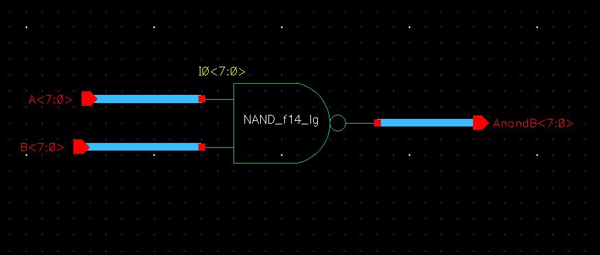
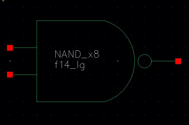
8-bit NAND
Schematic
Symbol
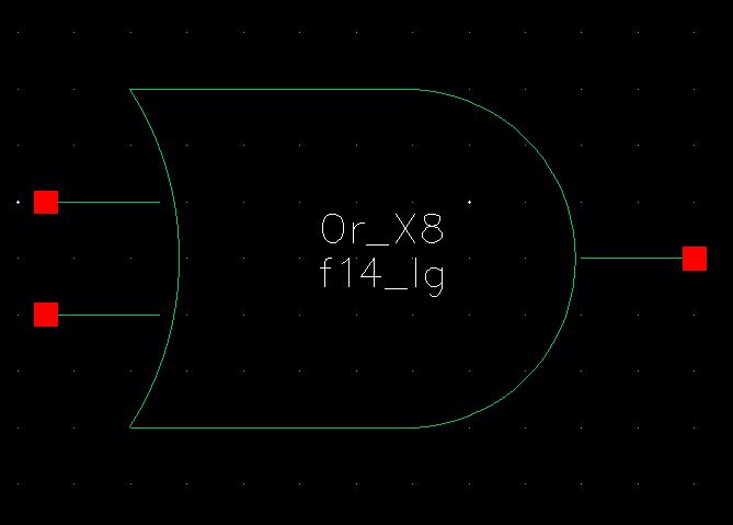
8-bit Or
Schematic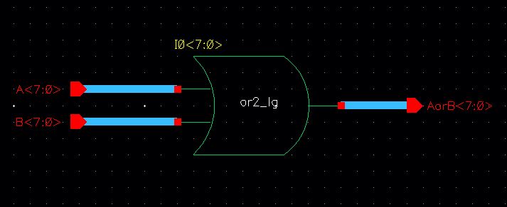
Symbol
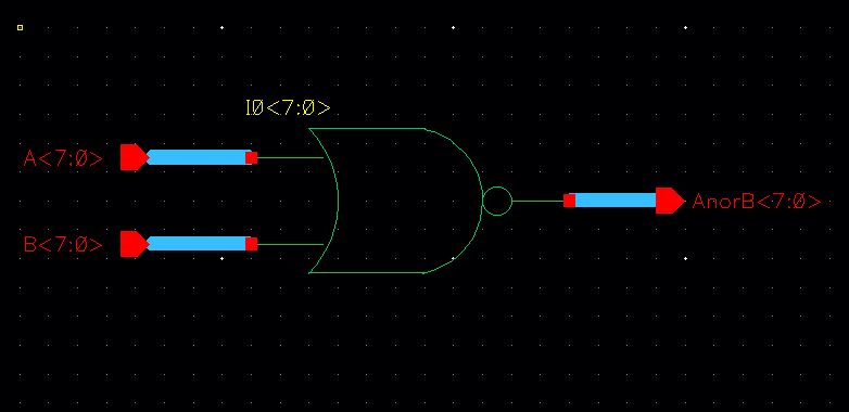
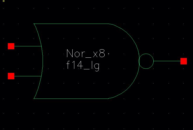
8-bit Nor
Schematic
Symbol
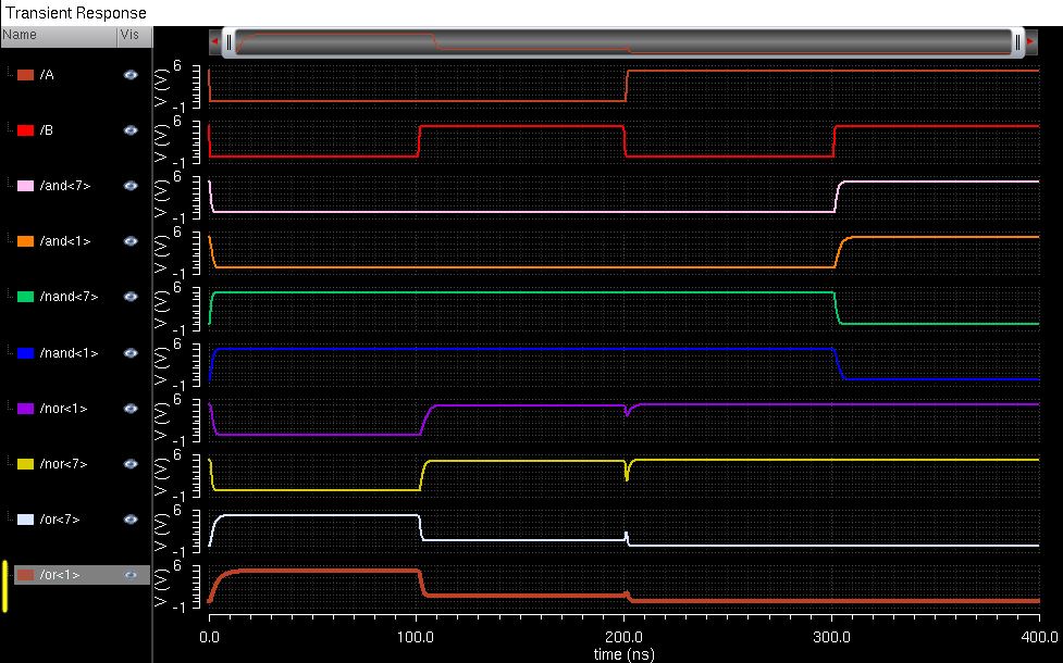
Gate Simulation
To trouble shoot simulation errors its best to simulate the gates individually.
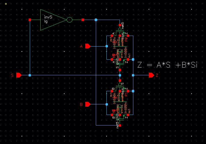
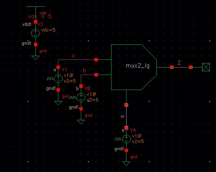
1-Bit Mux
Schematic
The
lab instructions state to remove the Si input pin from the Mux symbol.
To do that we inverted the S pin to get Si. (Note: the schematic will
not work if the inverter pins are other values besides S and Si)
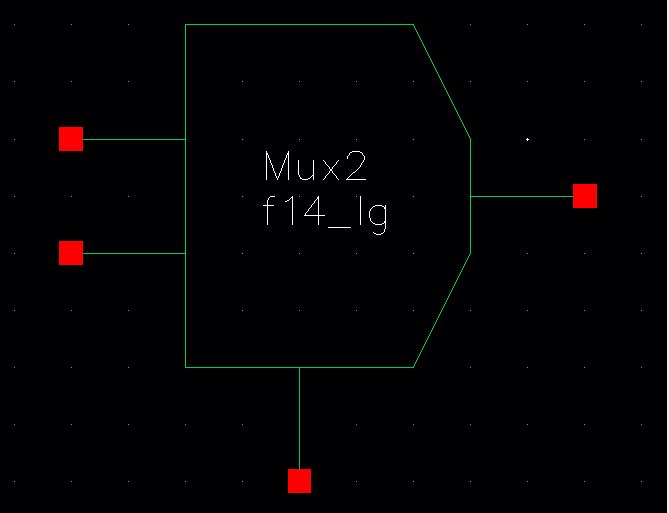
Symbol
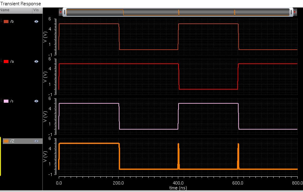
Simulation
Let's ensure that the symbol works properly before creating an 8-bit Mux
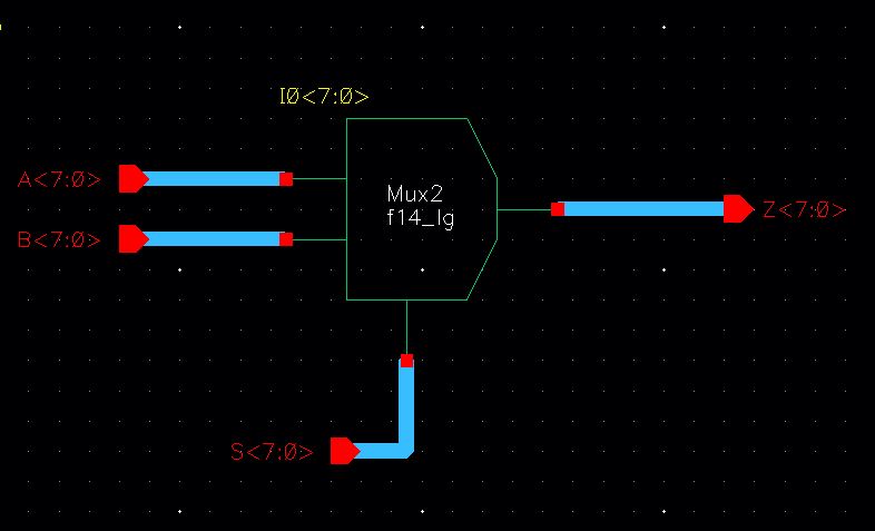
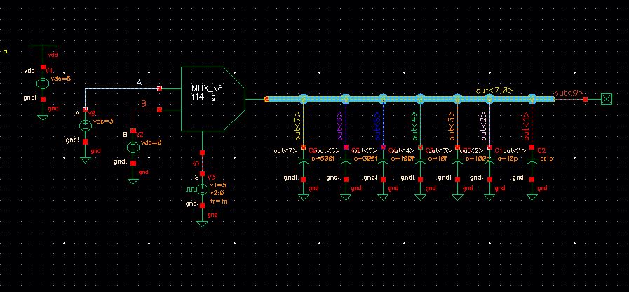
8-bit Mux
Schematic
Use the same techniques from earlier
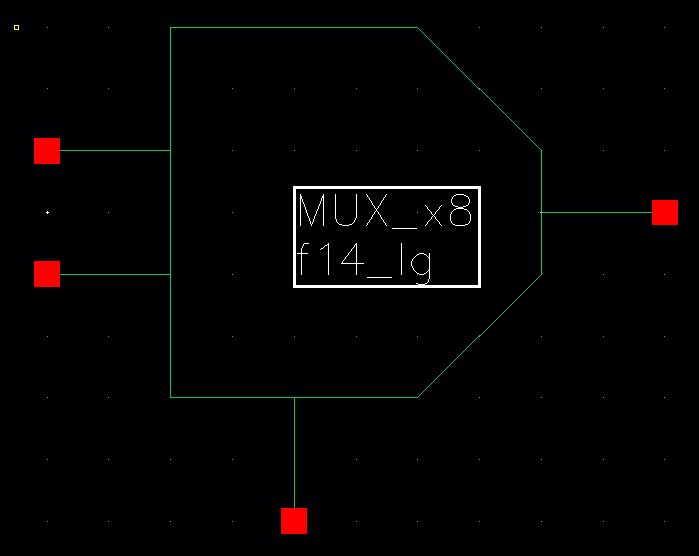
Symbol
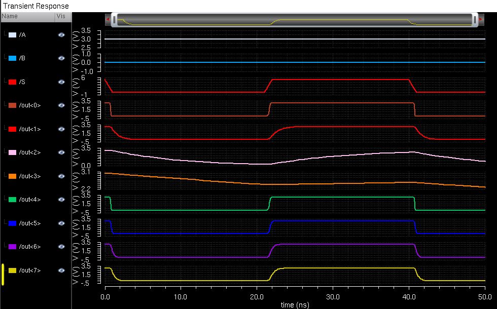
Simulation
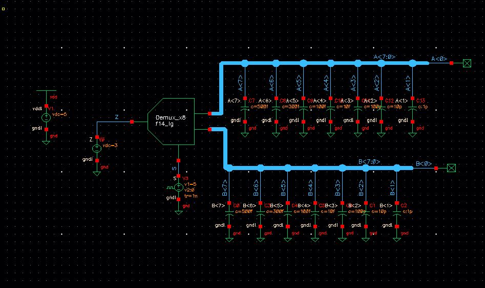
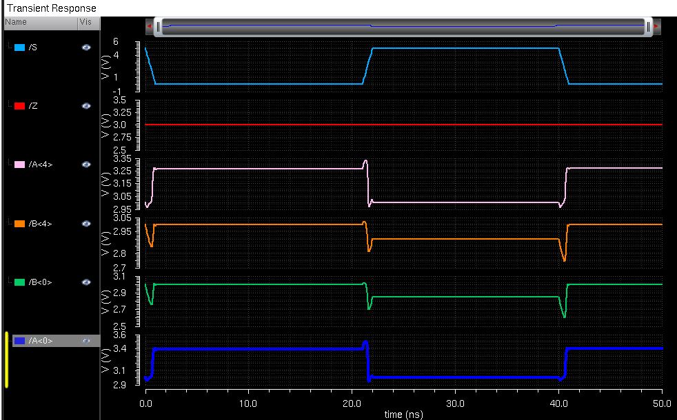
8-bit Demux
To create a Demux from Mux just change the pins A and B to an Output and Z into an Input
Schematic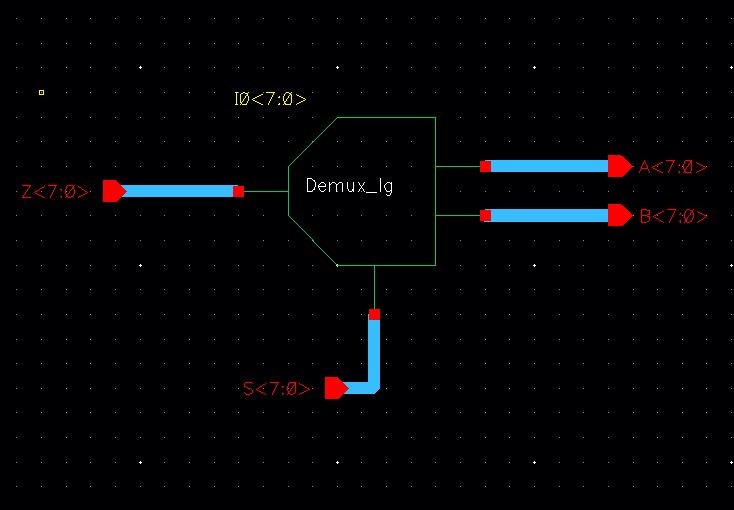
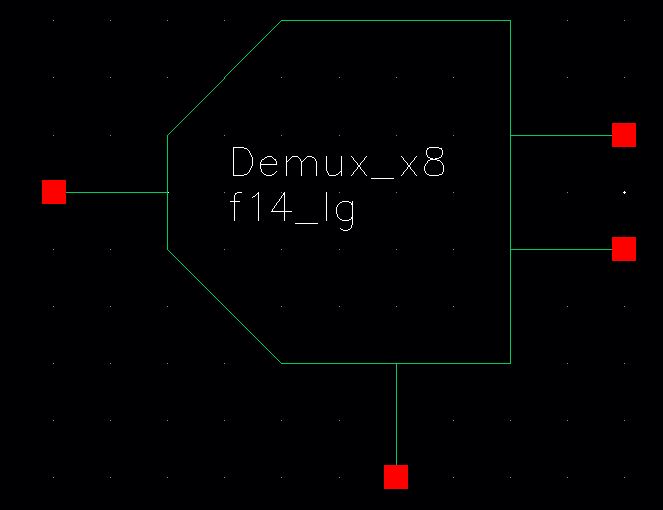
Symbol
Simulation
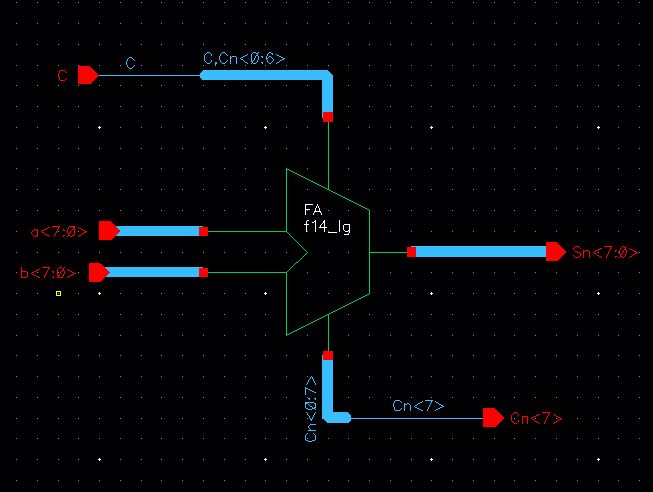
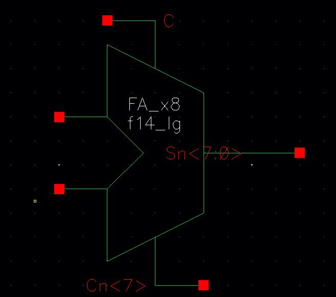
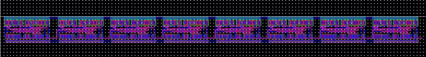
8-bit Full Adder
This concludes Lab 7.
Download and email the lab file for safe keeping
lab directory
Return to EE 421L